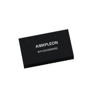
B11G3338N80D
Download datasheetLDMOS 3-stage integrated Doherty MMIC
The B11G3338N80D is a dual section 3-stage fully integrated Doherty MMIC solution using Ampleon's state of the art LDMOS technology. The carrier and peaking device, input splitter, output combiner and pre-match are integrated in each section. This multiband device is perfectly suited as general purpose driver in the frequency range 3300 MHz to 3800 MHz. Available in PQFN outline.
Features and benefits
- Integrated input splitter
- Integrated output combiner
- 25 Ω output impedance thanks to integrated pre-match
- Designed for wideband operation
- High linearity
- Independent control of carrier and peaking bias
- Integrated ESD protection
- Integrated bias gate switch
- Source impedance 50 Ω; high power gain
- For RoHS compliance see the product details on the Ampleon website
Applications
- Macrocell base station driver
- Microcell base station
- 5G mMIMO
- W-CDMA/LTE
- Active antenna
- General purpose applications
Parametrics
| Symbol | Parameter | Conditions | Min | Typ/Nom | Max | Unit |
|---|---|---|---|---|---|---|
| frange | frequency range | 3300 | 3800 | MHz | ||
| PL(3dB) | nominal output power at 3 dB gain compression | 75 | W | |||
| Test signal: Pulsed CW | ||||||
| VDS | drain-source voltage | [0] [1] | 28 | V | ||
| Gp | power gain | PL = 5 W (37 dBm) [0] [1] | 31 | 34 | 38 | dB |
| ηD | drain efficiency | PL = PL(3dB) [0] [1] | 30 | 40 | % | |
| ηD | drain efficiency | PL = 5 W (37 dBm) [0] [1] | 18 | 25 | % | |
| RLin | input return loss | [0] [1] | -15 | -10 | dB | |
Package / Packing
All type numbers in the table below are discontinued.
| Type number |
Package type, (Package outline) |
Outline version | Packing | Product status | Marking |
Orderable part number, (Ordering code (12NC)) |
|---|---|---|---|---|---|---|
| B11G3338N80D | PQFN-12x7 (PQFN-12x7-36-1) |
pqfn-12x7-36-1_po | TR13; 1500-fold; 24 mm; dry pack | Discontinued | Standard Marking |
B11G3338N80DX (9349 604 70525) |
| TR7; 300-fold; 24 mm; dry pack | Discontinued | Standard Marking |
B11G3338N80DYZ (9349 604 70535) |
Discontinuation information
Pinning info
| Pin | Symbol | Description | Simplified outline | Graphic symbol |
|---|---|---|---|---|
| 1 | GND | ground |
|
|
| 2 | VDS2_A/decoupling | drain-source voltage of final stages of section A | ||
| 3 | c.t.g. | connect to ground | ||
| 4 | VGS(carr) | gate-source voltage of carrier | ||
| 5 | VGS(peak) | gate-source voltage of peaking | ||
| 6 | VDS1_A | drain-source voltage of driver stages of section A | ||
| 7 | GND | ground | ||
| 8 | n.c. | not connected | ||
| 9 | PA_e | PA enable trigger signal, 0 V to 5 V, IDq-bias ON/OFF corresponds to logic HIGH/LOW | ||
| 10 | VDD(5V) | supply voltage (5 V) | ||
| 11 | GND | ground | ||
| 12 | RF_IN_A | RF input of section A | ||
| 13 | GND | ground | ||
| 14 | RF_IN_B | RF input of section B | ||
| 15 | GND | ground | ||
| 16 | VDD(5V) | supply voltage (5 V) | ||
| 17 | PA_e | PA enable trigger signal, 0 V to 5 V, IDq-bias ON/OFF corresponds to logic HIGH/LOW | ||
| 18 | n.c. | not connected | ||
| 19 | GND | ground | ||
| 20 | VDS1_B | drain-source voltage of driver stages of section B | ||
| 21 | VGS(peak) | gate-source voltage of peaking | ||
| 22 | VGS(carr) | gate-source voltage of carrier | ||
| 23 | c.t.g. | connect to ground | ||
| 24 | VDS2_B/decoupling | drain-source voltage of final stages of section B | ||
| 25 | GND | ground | ||
| 26, 27, 28, 29, 30 | RF_OUT_B | RF output of section B | ||
| 31 | GND | ground | ||
| 32, 33, 34, 35, 36 | RF_OUT_A | RF output of section A |
Documentation
| Title | Type | Date | |
|---|---|---|---|
| LDMOS 3-stage integrated Doherty MMIC | Data sheet | 2022-04-07 | |
| Mounting and soldering of RF transistors in overmolded plastic packages | Application note | 2025-02-03 | |
| Packages for RF power transistors | Leaflet | 2026-04-17 | |
| RF power solutions for Wireless Infrastructure | Brochure | 2026-04-20 |
Design support
| Title | Type | Date | |
|---|---|---|---|
| Printed-Circuit Board (PCB) B11G3338N80D (Data sheet) | Design support | 2022-01-19 |