
BLM6G22-30G
Download datasheetBLM6G22-30G
Download datasheet
This product has been discontinued.
Click here for discontinuation information.
The replacement is: BLM7G1822S-40PBG
The replacement is: BLM7G1822S-40PBG
W-CDMA 2100 MHz to 2200 MHz power MMIC
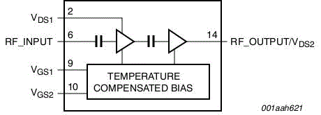
30 W LDMOS 2-stage power MMIC for base station applications at frequencies from 2100 MHz to 2200 MHz. Available in gull wing for surface mount (SOT822-1) or flat lead (SOT834-1).
Features and benefits
- Excellent thermal stability
- Biasing of individual stages is externally accessible
- High power gain
- Integrated ESD protection
- Integrated temperature compensated bias
- On-chip matching (input matched to 50 Ohm, output partially matched)
- Designed for broadband operation (2100 MHz to 2200 MHz)
- Small component size, very suitable for PA size reduction
- Compliant to Directive 2002/95/EC, regarding RoHS
Applications
- base station applications
Parametrics
| Symbol | Parameter | Conditions | Min | Typ/Nom | Max | Unit |
|---|---|---|---|---|---|---|
| Section-0 | ||||||
| frange | frequency range | 2100 | 2200 | MHz | ||
| PL(3dB) | nominal output power at 3 dB gain compression | 30 | W | |||
| Test-signal--2-c-W-CDMA | ||||||
| Gp | power gain | PL(AV) = 2 W; VDS = 28 V | 27.5 | 29.5 | 32.5 | dB |
| RLin | input return loss | PL(AV) = 2 W; VDS = 28 V; IDq = 270 mA | -14 | -10 | dB | |
| ηD | drain efficiency | PL(AV) = 2 W; VDS = 28 V; 2100 MHz < f < 2200 MHz; IDq = 270 mA | 7.5 | 9 | % | |
| PL(AV) | average output power | 2 | W | |||
| IMD3 | third-order intermodulation distortion | PL(AV) = 2 W; VDS = 28 V | -48 | -44.5 | dBc | |
| ACPR | adjacent channel power ratio | PL(AV) = 2 W; VDS = 28 V; 2100 MHz < f < 2200 MHz; IDq = 270 mA | -50 | -47 | dB | |
Package / Packing
All type numbers in the table below are discontinued.
| Type number |
Package type, (Package outline) |
Outline version | Packing | Product status | Marking |
Orderable part number, (Ordering code (12NC)) |
|---|---|---|---|---|---|---|
| BLM6G22-30G | SOT822 (SOT822-1) |
sot822-1_po | Reel 13" Q1/T1 | Withdrawn | Standard Marking |
BLM6G22-30G,118 (934060304118) |
| Reel 11¼" Q1/T1 in LargePack | Withdrawn | Standard Marking |
BLM6G22-30G,135 (934060304135) |
Discontinuation information
| Type number | 12NC | OPN | LTB date | LTD date | Replacement | DN notice | Product status |
|---|---|---|---|---|---|---|---|
| BLM6G22-30G | 934060304118 | BLM6G22-30G,118 | 2017-03-31 | 2017-06-30 | BLM7G1822S-40PBG | 201606001DN | Withdrawn |
| BLM6G22-30G | 934060304135 | BLM6G22-30G,135 | 2017-03-31 | 2017-06-30 | BLM7G1822S-40PBG | 201606001DN | Withdrawn |
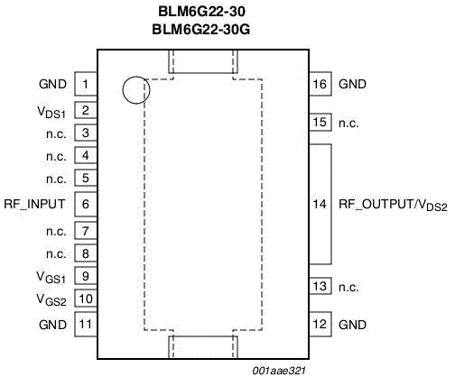
Pinning info
| Pin | Symbol | Description | Simplified outline | Graphic symbol |
|---|---|---|---|---|
| 1 | GND | ground |
|
|
| 2 | VDS1 | first stage drain-source voltage | ||
| 3 | n.c. | not connected | ||
| 4 | n.c. | not connected | ||
| 5 | n.c. | not connected | ||
| 6 | RF_INPUT | RF input | ||
| 7 | n.c. | not connected | ||
| 8 | n.c. | not connected | ||
| 9 | VGS1 | first stage gate-source voltage | ||
| 10 | VGS2 | second stage gate-source voltage | ||
| 11 | GND | ground | ||
| 12 | GND | ground | ||
| 13 | n.c. | not connected | ||
| 14 | RF_OUT/VDS2 | RF output or second stage drain-source voltage | ||
| 15 | n.c. | not connected | ||
| 16 | GND | ground | ||
| flange | RF_GND | RF ground |
Documentation
| Title | Type | Date | |
|---|---|---|---|
| W-CDMA 2100 MHz to 2200 MHz power MMIC | Data sheet | 2015-12-07 | |
| Mounting and soldering of RF transistors in overmolded plastic packages | Application note | 2025-02-03 | |
| Packages for RF power transistors | Leaflet | 2026-04-17 | |
| RF power solutions for Wireless Infrastructure | Brochure | 2026-06-15 |
Design support
| Title | Type | Date | |
|---|---|---|---|
| Printed-Circuit Board (PCB) BLM6G22-30(G) (Data sheet) | Design support | 2012-02-24 |