
BLF7G27LS-75P
Download datasheetPower LDMOS transistor
75 W LDMOS power transistor for base station applications at frequencies from 2300 MHz to 2700 MHz.
Features and benefits
- Designed for low memory effects providing excellent pre-distortability
- Internally matched for ease of use
- Excellent ruggedness
- Integrated ESD protection
- High efficiency
- Designed for broadband operation (2300 MHz to 2700 MHz)
- Low Rth providing excellent thermal stability
- Lower output capacitance for improved performance in Doherty applications
- Compliant to Directive 2002/95/EC, regarding Restriction of Hazardous Substances
Applications
- RF power amplifiers for W-CDMA base stations and multi carrier applications
Parametrics
| Symbol | Parameter | Conditions | Min | Typ/Nom | Max | Unit |
|---|---|---|---|---|---|---|
| frange | frequency range | 2300 | 2700 | MHz | ||
| PL(3dB) | nominal output power at 3 dB gain compression | 75 | W | |||
| Test signal: NCDMA/IS95 | ||||||
| Gp | power gain | PL(AV) = 12 W; VDS = 28 V | 15.8 | 17 | dB | |
| RLin | input return loss | PL(AV) = 12 W; VDS = 28 V; IDq = 650 mA | -12 | -8 | dB | |
| ηD | drain efficiency | PL(AV) = 12 W; VDS = 28 V; 2300 MHz ≤ f ≤ 2400 MHz; IDq = 650 mA | 23 | 26 | % | |
| PL(AV) | average output power | 12 | W | |||
| ACPR885k | adjacent channel power ratio (885 kHz) | PL(AV) = 12 W; VDS = 28 V; 2300 MHz ≤ f ≤ 2400 MHz; IDq = 650 mA | -46 | -42 | dBc | |
Package / Packing
All type numbers in the table below are discontinued.
| Type number |
Package type, (Package outline) |
Outline version | Packing | Product status | Marking |
Orderable part number, (Ordering code (12NC)) |
|---|---|---|---|---|---|---|
| BLF7G27LS-75P | ACC-780 (SOT1121B) |
sot1121b_po | Bulk Pack | Withdrawn | Standard Marking |
BLF7G27LS-75P,112 (9340 645 58112) |
| Reel 13" Q1/T1 | Withdrawn | Standard Marking |
BLF7G27LS-75P,118 (9340 645 58118) |
Discontinuation information
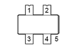
Pinning info
| Pin | Symbol | Description | Simplified outline | Graphic symbol |
|---|---|---|---|---|
| 1 | DRAIN1 | drain 1 |
|

|
| 2 | DRAIN2 | drain 2 | ||
| 3 | GATE1 | gate 1 | ||
| 4 | GATE2 | gate 2 | ||
| 5 | SOURCE | source |
Documentation
| Title | Type | Date | |
|---|---|---|---|
| Power LDMOS transistor | Data sheet | 2015-12-07 | |
| Mounting and soldering of RF transistors in air cavity packages | Application note | 2025-02-03 | |
| Packages for RF power transistors | Leaflet | 2025-06-20 | |
| RF power solutions for Wireless Infrastructure | Brochure | 2025-08-08 |
No documentation available.