
BLM7G1822S-40AB
Download datasheetLDMOS 2-stage power MMIC
The BLM7G1822S-40AB(G) is a dual section, asymmetric, 2-stage power MMIC using Ampleon’s state of the art GEN7 LDMOS technology. This multiband device is perfectly suited as small cell final in Doherty configuration, or as general purpose driver in the 1805 MHz to 2170 MHz frequency range. Available in gull wing or straight lead outline.
Features and benefits
- Designed for broadband operation (frequency 1805 MHz to 2170 MHz)
- High section-to-section isolation enabling multiple combinations
- High Doherty efficiency thanks to 2 : 1 asymmetry
- Integrated temperature compensated bias
- Biasing of individual stages is externally accessible
- Integrated ESD protection
- Excellent thermal stability
- High power gain
- On-chip matching for ease of use
- Compliant to Directive 2002/95/EC, regarding restriction of hazardous substances (RoHS)
Applications
-
RF power MMIC for W-CDMA base stations in the 1805 MHz to 2170 MHz frequency range. Possible
circuit topologies are the following:
- Asymmetric final stage in Doherty configuration
- Asymmetric driver for high power Doherty amplifier
Parametrics
| Symbol | Parameter | Conditions | Min | Typ/Nom | Max | Unit |
|---|---|---|---|---|---|---|
| frange | frequency range | 1805 | 2170 | MHz | ||
| PL(3dB) | nominal output power at 3 dB gain compression | 40 | W | |||
| Test signal: 1-c W-CDMA, Peaking section | ||||||
| Gp | power gain | VDS = 28 V; f = 2167.5 MHz [0] | 30 | 31.5 | 33 | dB |
| Gp | power gain | VDS = 28 V; f = 1807.5 MHz [0] | 31.3 | dB | ||
| RLin | input return loss | VDS = 28 V; f = 2167.5 MHz [0] | -20 | -10 | dB | |
| ηD | drain efficiency | VDS = 28 V; f = 2167.5 MHz [0] | 22 | 26.5 | % | |
| ηD | drain efficiency | VDS = 28 V; f = 1807.5 MHz [0] | 25.5 | % | ||
| ACPR5M | adjacent channel power ratio (5 MHz) | VDS = 28 V; f = 2167.5 MHz [0] | -38 | -34 | dB | |
| ACPR5M | adjacent channel power ratio (5 MHz) | VDS = 28 V; f = 1807.5 MHz [0] | -41 | dB | ||
| PARO | peak-to-average ratio output | f = 2167.5 MHz [0] | 6.5 | 7.9 | dB | |
| PARO | peak-to-average ratio output | f = 1807.5 MHz [0] | 8.2 | dB | ||
| Test signal: 1-c W-CDMA, Carrier section | ||||||
| Gp | power gain | VDS = 28 V; f = 2167.5 MHz [0] | 30 | 31.5 | 33 | dB |
| Gp | power gain | VDS = 28 V; f = 1807.5 MHz [0] | 31.8 | dB | ||
| RLin | input return loss | VDS = 28 V; f = 2167.5 MHz [0] | -15 | -10 | dB | |
| ηD | drain efficiency | VDS = 28 V; f = 2167.5 MHz [0] | 21 | 25.5 | % | |
| ηD | drain efficiency | VDS = 28 V; f = 1807.5 MHz [0] | 18 | % | ||
| ACPR5M | adjacent channel power ratio (5 MHz) | VDS = 28 V; f = 2167.5 MHz [0] | -37 | -33 | dBc | |
| ACPR5M | adjacent channel power ratio (5 MHz) | VDS = 28 V; f = 1807.5 Hz [0] | -39 | dBc | ||
| PARO | output peak-to-average ratio | f = 2167.5 MHz [0] | 6.4 | 7.7 | dB | |
| PARO | output peak-to-average ratio | f = 1807.5 MHz [0] | 8.4 | dB | ||
Package / Packing
All type numbers in the table below are discontinued.
| Type number |
Package type, (Package outline) |
Outline version | Packing | Product status | Marking |
Orderable part number, (Ordering code (12NC)) |
|---|---|---|---|---|---|---|
| BLM7G1822S-40AB | OMP-780 (SOT1211-2) |
sot1211-2_po | Reel 13" Q1/T1 in Drypack | Withdrawn | Standard Marking |
BLM7G1822S-40ABY (934068895518) |
Discontinuation information
Pinning info
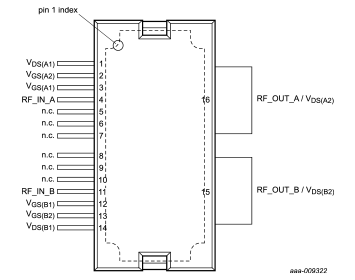
| Pin | Symbol | Description | Simplified outline | Graphic symbol |
|---|---|---|---|---|
| 1 | VDS(A1) | drain-source voltage of carrier section, driver stage (A1) |
|
|
| 2 | VGS(A2) | gate-source voltage of carrier section, final stage (A2) | ||
| 3 | VGS(A1) | gate-source voltage of carrier section, driver stage (A1) | ||
| 4 | RF_IN_A | RF input carrier section (A) | ||
| 5 | n.c. | not connected | ||
| 6 | n.c. | not connected | ||
| 7 | n.c. | not connected | ||
| 8 | n.c. | not connected | ||
| 9 | n.c. | not connected | ||
| 10 | n.c. | not connected | ||
| 11 | RF_IN_B | RF input peaking section (B) | ||
| 12 | VGS(B1) | gate-source voltage of peaking section, driver stage (B1) | ||
| 13 | VGS(B2) | gate-source voltage of peaking section, final stage (B2) | ||
| 14 | VDS(B1) | drain-source voltage of peaking section, driver stage (B1) | ||
| 15 | RF_OUT_B/VDS(B2) | RF output peaking section (B) / drain-source voltage of peaking section, final stage (B2) | ||
| 16 | RF_OUT_A/VDS(A2) | RF output carrier section (A) / drain-source voltage of carrier section, final stage (A2) | ||
| flange | GND | RF ground |
Documentation
| Title | Type | Date | |
|---|---|---|---|
| Mounting and soldering of RF transistors in overmolded plastic packages | Application note | 2025-02-03 | |
| LDMOS 2-stage power MMIC | Data sheet | 2015-12-07 | |
| Biasing asymmetrical Doherty RF power transistor | Other type | 2016-08-31 | |
| Packages for RF power transistors | Leaflet | 2026-04-17 | |
| RF power solutions for Wireless Infrastructure | Brochure | 2026-06-15 |
Design support
| Title | Type | Date | |
|---|---|---|---|
| Printed-Circuit Board (PCB) BLM7G1822S-40AB(G) (Data sheet) | Design support | 2015-07-20 |