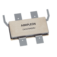
C4H27W400AV
Request datasheetThis product is not recommended for design-in.
The recommended type is: C4H27P400A
C4H27W400AV
Request datasheetThis product is not recommended for design-in.
The recommended type is: C4H27P400A
Power GaN transistor
400 W GaN packaged asymmetric Doherty power transistor for base station applications at frequencies from 2300 MHz to 2700 MHz.
Features and benefits
- Excellent digital pre-distortion capability
- High efficiency
- Designed for broadband operation
- Lower output capacitance for improved performance in Doherty applications
- Internally matched for ease of use
- For RoHS compliance see the product details on the Ampleon website
Applications
- RF power amplifier for base stations and multi carrier applications in the 2300 MHz to 2700 MHz frequency range
Parametrics
| Symbol | Parameter | Conditions | Min | Typ/Nom | Max | Unit |
|---|---|---|---|---|---|---|
| frange | frequency range | 2300 | 2690 | MHz | ||
| PL(3dB) | nominal output power at 3 dB gain compression | 400 | W | |||
| Test signal: 1-c W-CDMA | ||||||
| VDS | drain-source voltage | f = 2496 MHz to 2690 MHz [0] [1] | 50 | V | ||
| Gp | power gain | f = 2496 MHz to 2690 MHz [0] [1] | 15.4 | dB | ||
| ηD | drain efficiency | f = 2496 MHz to 2690 MHz [0] [1] | 53.7 | % | ||
| PL(AV) | average output power | f = 2496 MHz to 2690 MHz [0] [1] | 47.2 | dBm | ||
| IDq | quiescent drain current | f = 2496 MHz to 2690 MHz [0] [1] | 200 | mA | ||
| ACPR | adjacent channel power ratio | f = 2496 MHz to 2690 MHz [0] [1] | -27 | dBc | ||
Package / Packing
All type numbers in the table below are not recommended for design-in.
| Type number |
Package type, (Package outline) |
Outline version | Packing | Product status | Marking |
Orderable part number, (Ordering code (12NC)) |
|---|---|---|---|---|---|---|
| C4H27W400AV | ACP-780 (SOT1275-1) |
sot1275-1_po | Tray; 20-fold; dry pack | Active | Standard Marking |
C4H27W400AVZ (934960485517) |
| TR13; 100-fold; 44 mm; dry pack | Active | Standard Marking |
C4H27W400AVY (934960485518) |
Pinning info
| Pin | Symbol | Description | Simplified outline | Graphic symbol |
|---|---|---|---|---|
| 1 | D1 | drain 1 (main) |

|
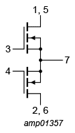
|
| 2 | D2 | drain2 (peak) | ||
| 3 | G1 | gate 1 (main) | ||
| 4 | G2 | gate 2 (peak) | ||
| 5 | VD | video decoupling (main) | ||
| 6 | VD | video decoupling (peak) | ||
| 7 | S | source |
Documentation
| Title | Type | Date | |
|---|---|---|---|
| Mounting and soldering of RF transistors in air cavity packages | Application note | 2025-02-03 | |
| Thermal characteristics of GaN power transistors | Application note | 2024-09-01 | |
| Packages for RF power transistors | Leaflet | 2026-04-17 | |
| RF power solutions for Wireless Infrastructure | Brochure | 2026-06-15 |
No documentation available.