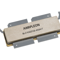
BLC10G27XS-400AVT
Download datasheetThis product is not recommended for design-in.
Power LDMOS transistor
400 W LDMOS packaged asymmetric Doherty power transistor for base station applications at frequencies from 2496 MHz to 2690 MHz.
Features and benefits
- Excellent ruggedness
- High efficiency
- Low thermal resistance providing excellent thermal stability
- Lower output capacitance for improved performance in Doherty applications
- Designed for low memory effects providing excellent digital pre-distortion capability
- Internally matched for ease of use
- Integrated ESD protection
- For RoHS compliance see the product details on the Ampleon website
Applications
- RF power amplifiers for base stations and multi carrier applications in the 2496 MHz to 2690 MHz frequency range
Parametrics
| Symbol | Parameter | Conditions | Min | Typ/Nom | Max | Unit |
|---|---|---|---|---|---|---|
| frange | frequency range | 2496 | 2690 | MHz | ||
| PL(3dB) | nominal output power at 3 dB gain compression | 430 | W | |||
| Test signal: 1-c W-CDMA | ||||||
| VDS | drain-source voltage | PL(AV) = 56.2 W [0] | 28 | V | ||
| Gp | power gain | PL(AV) = 56.2 W [0] | 12.4 | 13.3 | dB | |
| ηD | drain efficiency | PL(AV) = 56.2 W [0] | 41 | 45 | % | |
| ACPR | adjacent channel power ratio | PL(AV) = 56.2 W [0] | -28 | -24 | dBc | |
| RLin | input return loss | PL(AV) = 56.2 W [0] | -11 | -7 | dB | |
Package / Packing
All type numbers in the table below are not recommended for design-in.
| Type number |
Package type, (Package outline) |
Outline version | Packing | Product status | Marking |
Orderable part number, (Ordering code (12NC)) |
|---|---|---|---|---|---|---|
| BLC10G27XS-400AVT | ACP-1230 (SOT1258-4) |
sot1258-4_po | Reel 13" Q1/T1 in Drypack | Active | Standard Marking |
BLC10G27XS-400AVTY (934960323518) |
| Tray, NonBakeable, Multiple in Drypack | Active | Standard Marking |
BLC10G27XS-400AVTZ (934960323517) |
Pinning info
| Pin | Symbol | Description | Simplified outline | Graphic symbol |
|---|---|---|---|---|
| 1 | D2P | drain2 (peak) |
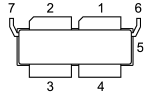
|

|
| 2 | D1M | drain1 (main) | ||
| 3 | G1M | gate1 (main) | ||
| 4 | G2P | gate2 (peak) | ||
| 5 | S | source [1] | ||
| 6 | VDP | video decoupling (peak) | ||
| 7 | VDM | video decoupling (main) |
Documentation
| Title | Type | Date | |
|---|---|---|---|
| Power LDMOS transistor | Data sheet | 2021-06-24 | |
| Mounting and soldering of RF transistors in air cavity packages | Application note | 2025-02-03 | |
| Packages for RF power transistors | Leaflet | 2026-04-17 | |
| RF power solutions for Wireless Infrastructure | Brochure | 2026-06-15 |
Design support
| Title | Type | Date | |
|---|---|---|---|
| Printed-Circuit Board (PCB) BLC10G27XS-400AVT (Data sheet) | Design support | 2021-06-24 | |
| BLC10G27XS-400AVT Model for ADS 2019 (Keysight Advanced Design System) | Simulation model | 2021-10-27 |