BLC10G19LS-250WT
Download datasheetPower LDMOS transistor
250 W LDMOS power transistor for base station applications at frequencies from 1930 MHz to 1990 MHz.
Features and benefits
- Excellent ruggedness
- Excellent video bandwidth enabling full band operation
- High efficiency
- Low thermal resistance providing excellent thermal stability
- Designed for low memory effects providing excellent pre-distortability
- Device can operate with the supply current delivered through video leads
- Internally matched for ease of use
- Integrated ESD protection
- Compliant to Directive 2002/95/EC, regarding Restriction of Hazardous Substances (RoHS)
Applications
- RF power amplifier for W-CDMA base stations and multi carrier applications in the 1930 MHz to 1990 MHz frequency range
Parametrics
| Symbol | Parameter | Conditions | Min | Typ/Nom | Max | Unit |
|---|---|---|---|---|---|---|
| frange | frequency range | 1930 | 1990 | MHz | ||
| PL(3dB) | nominal output power at 3 dB gain compression | 250 | W | |||
| Test signal: 2-c W-CDMA | ||||||
| VDS | drain-source voltage | 1930 to 1990 MHz [0] | 28 | V | ||
| Gp | power gain | 1930 to 1990 MHz [0] | 19.3 | dB | ||
| ηD | drain efficiency | 1930 to 1990 MHz [0] | 31 | % | ||
| PL(AV) | average output power | 1930 to 1990 MHz [0] | 60 | W | ||
| IDq | quiescent drain current | 1930 to 1990 MHz [0] | 1400 | mA | ||
| ACPR | adjacent channel power ratio | 1930 to 1990 MHz [0] | -31 [1] | dBc | ||
Package / Packing
All type numbers in the table below are discontinued.
| Type number |
Package type, (Package outline) |
Outline version | Packing | Product status | Marking |
Orderable part number, (Ordering code (12NC)) |
|---|---|---|---|---|---|---|
| BLC10G19LS-250WT | ACP-780 (SOT1271-2) |
sot1271-2_po | Reel 13" Q1/T1 | Discontinued | Standard Marking |
BLC10G19LS-250WTY (934960075518) |
| Bulk Pack | Discontinued | Standard Marking |
BLC10G19LS-250WTZ (934960075517) |
Discontinuation information
Pinning info
| Pin | Symbol | Description | Simplified outline | Graphic symbol |
|---|---|---|---|---|
| 1 | D | drain |
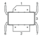
|

|
| 2 | G | gate | ||
| 3 | S | source [2] | ||
| 4 | VD | video decoupling | ||
| 5 | VD | video decoupling | ||
| 6 | n.c | not connected | ||
| 7 | n.c | not connected |
Documentation
| Title | Type | Date | |
|---|---|---|---|
| Power LDMOS transistor | Data sheet | 2017-10-19 | |
| Mounting and soldering of RF transistors in air cavity packages | Application note | 2025-02-03 | |
| Packages for RF power transistors | Leaflet | 2026-04-17 | |
| RF power solutions for Wireless Infrastructure | Brochure | 2026-06-15 |
Design support
| Title | Type | Date | |
|---|---|---|---|
| Printed-Circuit Board (PCB) BLC10G19LS-250WT (Data sheet) | Design support | 2017-10-26 |