B10G3438N55D
Download datasheetThis product is not recommended for design-in.
The recommended type is: G1M3438P70C (coming soon)
B10G3438N55D
Download datasheetThis product is not recommended for design-in.
The recommended type is: G1M3438P70C (coming soon)
LDMOS 3-stage integrated Doherty MMIC
The B10G3438N55D is a 3-stage fully integrated asymmetrical Doherty MMIC solution using Ampleon’s state of the art GEN10 LDMOS technology. The carrier and peaking device, input splitter, output combiner and pre-match are integrated in a single package. This multiband device is perfectly suited as a final stage for small cells and massive MIMO applications in the frequency range from 3400 MHz to 3800 MHz. Available in PQFN outline.
Features and benefits
- Integrated input splitter
- Integrated output combiner
- 30 Ω output impedance thanks to integrated pre-match
- Very high efficiency thanks to asymmetry
- Designed for wideband operation (frequency 3400 MHz to 3800 MHz)
- Independent control of carrier and peaking bias
- Integrated ESD protection
- Source impedance 50 Ω; high power gain
- For RoHS compliance see the product details on the Ampleon website
Parametrics
| Symbol | Parameter | Conditions | Min | Typ/Nom | Max | Unit |
|---|---|---|---|---|---|---|
| frange | frequency range | 3400 | 3800 | MHz | ||
| PL(3dB) | nominal output power at 3 dB gain compression | 55 | W | |||
| Test signal: Pulsed CW | ||||||
| VDS | drain-source voltage | [0] | 28 | V | ||
| Gp | power gain | PL = 7.94 W (39 dBm) [0] | 31.1 | 33.7 | 36.1 | dB |
| ηD | drain efficiency | PL = 7.94 W (39 dBm) [0] | 30 | 37.3 | % | |
| ηD | drain efficiency | PL = PL(3dB) [0] | 36 | 42 | % | |
| RLin | input return loss | [0] | -10 | dB | ||
Package / Packing
All type numbers in the table below are not recommended for design-in.
| Type number |
Package type, (Package outline) |
Outline version | Packing | Product status | Marking |
Orderable part number, (Ordering code (12NC)) |
|---|---|---|---|---|---|---|
| B10G3438N55D | PQFN-8x8 (SOT1462-1) |
sot1462-1_po | TR13; 500-fold; 16 mm; dry pack | Active | Standard Marking |
B10G3438N55DZ (9349 603 61515) |
Pinning info
| Pin | Symbol | Description | Simplified outline | Graphic symbol |
|---|---|---|---|---|
| 1 | VDS2/decoupling | drain-source voltage of final stages / video-lead for decoupling |
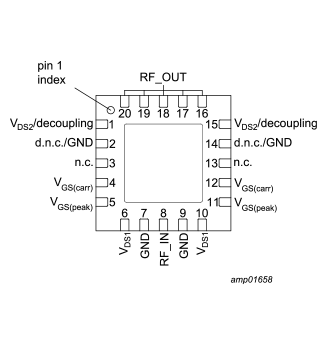
|
|
| 2 | d.n.c./GND | do not connect or GND | ||
| 3 | n.c. | not connected | ||
| 4 | VGS(carr) | gate-source voltage of carrier | ||
| 5 | VGS(peak) | gate-source voltage of peaking | ||
| 6 | VDS1 | drain-source voltage of driver stages | ||
| 7 | GND | RF ground | ||
| 8 | RF_IN | RF input | ||
| 9 | GND | RF ground | ||
| 10 | VDS1 | drain-source voltage of driver stages | ||
| 11 | VGS(peak) | gate-source voltage of peaking | ||
| 12 | VGS(carr) | gate-source voltage of carrier | ||
| 13 | n.c. | not connected | ||
| 14 | d.n.c./GND | do not connect or GND | ||
| 15 | VDS2/decoupling | drain-source voltage of final stages / video-lead for decoupling | ||
| 16 | RF_OUT | RF output | ||
| 17 | RF_OUT | RF output | ||
| 18 | RF_OUT | RF output | ||
| 19 | RF_OUT | RF output | ||
| 20 | RF_OUT | RF output | ||
| flange | GND | RF ground |
Documentation
| Title | Type | Date | |
|---|---|---|---|
| LDMOS 3-stage integrated Doherty MMIC | Data sheet | 2021-10-05 | |
| Mounting and soldering of RF transistors in overmolded plastic packages | Application note | 2025-02-03 | |
| Packages for RF power transistors | Leaflet | 2025-06-20 | |
| RF power solutions for Wireless Infrastructure | Brochure | 2025-08-08 |
Design support
| Title | Type | Date | |
|---|---|---|---|
| Printed-Circuit Board (PCB) B10G3438N55D (Data sheet) | Design support | 2021-10-07 |