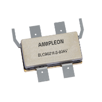
BLC9G21LS-60AV
Download datasheetThis product is not recommended for design-in.
Power LDMOS transistor
60 W LDMOS packaged asymmetric Doherty power transistor for base station applications at frequencies from 1805 MHz to 2200 MHz.
Features and benefits
- Excellent ruggedness
- High efficiency
- Low thermal resistance providing excellent thermal stability
- Asymmetric design to achieve optimum efficiency across the band
- Lower output capacitance for improved performance in Doherty applications
- Designed for low memory effects providing excellent digital pre-distortion
- Internally matched for ease of use
- Integrated ESD protection
- Compliant to Directive 2002/95/EC, regarding Restriction of Hazardous Substances (RoHS)
Applications
- RF power amplifiers for base stations and multi carrier applications in the 1805 MHz to 2200 MHz frequency range
Parametrics
| Symbol | Parameter | Conditions | Min | Typ/Nom | Max | Unit |
|---|---|---|---|---|---|---|
| frange | frequency range | 1805 | 2200 | MHz | ||
| PL(3dB) | nominal output power at 3 dB gain compression | 60 | W | |||
| Test signal: 1-c W-CDMA | ||||||
| VDS | drain-source voltage | 1930 to 1990 MHz [0] | 28 | V | ||
| Gp | power gain | 1930 to 1990 MHz [0] | 17.5 | dB | ||
| ηD | drain efficiency | 1930 to 1990 MHz [0] | 30 | % | ||
| PL(AV) | average output power | 1930 to 1990 MHz [0] | 2.5 | W | ||
| ACPR | adjacent channel power ratio | 1930 to 1990 MHz [0] | -39 [1] | dBc | ||
Package / Packing
All type numbers in the table below are not recommended for design-in.
| Type number |
Package type, (Package outline) |
Outline version | Packing | Product status | Marking |
Orderable part number, (Ordering code (12NC)) |
|---|---|---|---|---|---|---|
| BLC9G21LS-60AV | ACP-780 (SOT1275-1) |
sot1275-1_po | Reel 13" Q1/T1 in Drypack | Active | Standard Marking |
BLC9G21LS-60AVY (9349 600 94518) |
| Tray, NonBakeable, Multiple in Drypack | Active | Standard Marking |
BLC9G21LS-60AVZ (9349 600 94517) |
Pinning info
| Pin | Symbol | Description | Simplified outline | Graphic symbol |
|---|---|---|---|---|
| 1 | D1 | drain1 (main) |
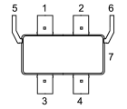
|

|
| 2 | D2 | drain2 (peak) | ||
| 3 | G1 | gate1 (main) | ||
| 4 | G2 | gate2 (peak) | ||
| 5 | VDM | video decoupling (main) | ||
| 6 | VDP | video decoupling (peak) | ||
| 7 | S | source [2] |
Documentation
| Title | Type | Date | |
|---|---|---|---|
| Power LDMOS transistor | Data sheet | 2017-07-06 | |
| Mounting and soldering of RF transistors in air cavity packages | Application note | 2025-02-03 | |
| Packages for RF power transistors | Leaflet | 2025-06-20 | |
| RF power solutions for Wireless Infrastructure | Brochure | 2025-08-08 |
Design support
| Title | Type | Date | |
|---|---|---|---|
| Printed-Circuit Board (PCB) BLC9G21LS-60AV (Data sheet) | Design support | 2017-12-28 |