BLP25RFE001
Download datasheetSignal generator for RF energy solutions
The product provides an all-in-one solution for the small signal generation in the RF energy solutions such as cooking and lighting markets.
The product facilitates RF energy design by:
- Allowing on-board integration
- Providing flexibility in system solution development
Features and benefits
- Support from 2400 MHz to 2483.5 MHz, from 902 MHz to 928 MHz and from 433 MHz to 434.8 MHz ISM bands
- Single 3.3 V supply voltage
- SPI-bus interface up to 20 MHz
- Fully integrated LC-VCO operating in the range from 6.6 GHz to 10 GHz and used with a Σ∆ PLL to generate the frequency
- Very fast tuning and hopping time PLL
- High frequency daisy chaining allowing coherent excitation of multiple RF amplifier chains
- 360° phase shifter with 1.4° steps
- Medium Power Amplifier (MPA) delivering an output up to +27 dBm peak power (max. +24 dBm for continuous use)
- Low Power Amplifier (PPA) delivering an output up to +7 dBm
- Integrated 20 dB gain control
- Integrated RF switch allowing PWM control
- Temperature sensor indicates the junction temperature of the die
- RoHS compliant
Applications
- Solid-state cooking
- Solid-state lighting
Parametrics
| Symbol | Parameter | Conditions | Min | Typ/Nom | Max | Unit | Function |
|---|---|---|---|---|---|---|---|
| frange | frequency range | 433 | 2500 | MHz | |||
| Test signal: CW @ 2450 MHz | |||||||
| frange | frequency range | 2400 | 2483.5 | MHz | PLL | ||
| tset | setting time | 50 | μs | PLL | |||
| ts(f) | frequency settling time | from one frequency to another | 5 | 10 | μs | PLL | |
| φn | phase noise | at 2483.5 MHz; at 100 kHz frequency offset | -87 | dBc/Hz | PLL | ||
| ∆φstep | phase shift step | 1.4 | ° | Phase shifter | |||
| φRF | RF phase | 0 | 360 | ° | Phase shifter | ||
| Eφ | phase error | absolute value step size error | 0 | 0.5 | 1 | ° | Phase shifter |
| Eφ | phase error | cumulative phase error | 5 | ° | Phase shifter | ||
| Po(max) | maximum output power | 24 | 27 | dBm | MPA | ||
| αsp(ob) | out-band spurious attenuation | consider second and third harmonics only | -30 | dBc | MPA | ||
| Pob | out-band power | integrated power outside the band of interest; fVCO(max) = frange max - 1 MHz; fVCO(min) = frange min + 1 MHz; rf_mpa_power[5:0] = 42 | -45 | dBc | MPA | ||
| Po(range) | output power range | 20 | dB | MPA | |||
| αisol | isolation | ON/OFF switch isolation | 40 | dB | MPA | ||
| tsw | switching time | OFF/ON ramping transition | 700 | ns | MPA | ||
| Zo | output impedance | 40 | Ω | MPA | |||
| Po(max) | maximum output power | rf_mpa_power[5:0] = 63 | 7 | dBm | PPA | ||
| Po | output power | rf_mpa_power[5:0] = 42 | 5 | dBm | PPA | ||
| Po(range) | output power range | 30 | dB | PPA | |||
| Zo | output impedance | 200 | Ω | PPA | |||
| Test signal: CW @ 915 MHz | |||||||
| frange | frequency range | 902 | 928 | MHz | PLL | ||
| tset | setting time | 50 | μs | PLL | |||
| ts(f) | frequency settling time | from one frequency to another | 5 | 10 | μs | PLL | |
| ∆αstep | phase shift step | 1.4 | ° | Phase shifter | |||
| φRF | RF phase | 0 | 360 | ° | Phase shifter | ||
| Eφ | phase error | absolute value step size error | 0 | 0.5 | 1 | ° | Phase shifter |
| Po(max) | maximum output power | 24 | 27 | dBm | MPA | ||
| Po(range) | output power range | 20 | dB | MPA | |||
| αisol | isolation | ON/OFF switch isolation | 40 | dB | MPA | ||
| tsw | switching time | OFF/ON ramping transition | 700 | ns | MPA | ||
| Zo | output impedance | 40 | Ω | MPA | |||
| Po(max) | maximum output power | rf_mpa_power[5:0] = 63 | 7 | dBm | PPA | ||
| Po | output power | 5 | dBm | PPA | |||
| Po(range) | output power range | 30 | dB | PPA | |||
| Zo | output impedance | 200 | Ω | PPA | |||
| Test signal: CW @ 433 MHz | |||||||
| frange | frequency range | 433.0 | 434.8 | MHz | PLL | ||
| tset | setting time | 50 | μs | PLL | |||
| ts(f) | frequency settling time | from one frequency to another | 5 | 10 | μs | PLL | |
| Po(max) | maximum output power | 24 | 27 | dBm | MPA | ||
| Po(range) | output power range | 20 | dB | MPA | |||
| αisol | isolation | ON/OFF switch isolation | 40 | dB | MPA | ||
| tsw | switching time | OFF/ON ramping transition | 700 | ns | MPA | ||
| Zo | output impedance | 40 | Ω | MPA | |||
| Po(max) | maximum output power | rf_mpa_power[5:0] = 63 | 7 | dBm | PPA | ||
| Po | output power | rf_mpa_power[5:0] = 42 | 5 | dBm | PPA | ||
| Po(range) | output power range | 30 | dB | PPA | |||
| Zo | output impedance | 200 | Ω | PPA | |||
Package / Packing
All type numbers in the table below are discontinued.
| Type number |
Package type, (Package outline) |
Outline version | Packing | Product status | Marking |
Orderable part number, (Ordering code (12NC)) |
|---|---|---|---|---|---|---|
| BLP25RFE001 | SOT993 (SOT993-3) |
sot993-3_po | Reel 13" Q1/T1 | Withdrawn | Standard Marking |
BLP25RFE001Y (934960173518) |
| Tray, NonBakeable, Multiple in Drypack | Withdrawn | Standard Marking |
BLP25RFE001E (934960173551) |
Discontinuation information
Pinning info
| Pin | Symbol | Description | Simplified outline | Graphic symbol |
|---|---|---|---|---|
| 1 | SSN | SPI-bus: Slave Select Not (from master) |
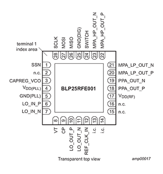
|
|
| 2 | n.c | not connected | ||
| 3 | CAPREG_VCO | VCO internal regulator filtering input | ||
| 4 | VDD(PLL) | PLL supply voltage; 3.3 V | ||
| 5 | GND(PLL) | PLL ground | ||
| 6 | LO_IN_P | high frequency daisy chaining positive input | ||
| 7 | LO_IN_N | high frequency daisy chaining negative input | ||
| 8 | VT | VCO input voltage | ||
| 9 | CP | charge pump output | ||
| 10 | LO_OUT_P | high frequency daisy chaining positive output | ||
| 11 | LO_OUT_N | high frequency daisy chaining negative output | ||
| 12 | REF_CLK_IN | external reference clock input | ||
| 13 | i.c. | internally connected | ||
| 14 | i.c. | internally connected | ||
| 15 | n.c. | not connected | ||
| 16 | n.c. | not connected | ||
| 17 | VDD(RF) | RF power supply; 3.3 V | ||
| 18 | PPA_OUT_P | RF low-power positive output | ||
| 19 | PPA_OUT_N | RF low-power negative output | ||
| 20 | MPA_LP_OUT_P | RF Intermediate supply for high-power first stage MPA positive path | ||
| 21 | MPA_LP_OUT_N | RF Intermediate supply for high-power first stage MPA negative path | ||
| 22 | MPA_HP_OUT_P | medium-power RF amplifier positive output | ||
| 23 | MPA_HP_OUT_N | medium-power RF amplifier negative output | ||
| 24 | SWITCH | RF switch control | ||
| 25 | GND(DIG) | digital ground | ||
| 26 | MISO | SPI-bus: Master Input Slave Output | ||
| 27 | MOSI | SPI-bus: Master Output Slave Input | ||
| 28 | SCLK | SPI-bus: Serial Clock (from master) | ||
| - | Exposed die pad | connect to RF ground |
Documentation
| Title | Type | Date | |
|---|---|---|---|
| Signal generator for RF energy solutions | Data sheet | 2018-01-26 | |
| Quick start OM3999 | Application note | 2018-04-23 | |
| Application note OM3999 | Application note | 2018-04-23 | |
| Programing user guide | Application note | 2018-04-23 | |
| RF power solutions for ISM, broadcast, navigation and safety radio applications | Brochure | 2026-04-17 | |
| RF power application reports for ISM, broadcast, navigation and safety radio applications | Brochure | 2026-04-17 | |
| Packages for RF power transistors | Leaflet | 2026-04-17 |
Design support
| Title | Type | Date | |
|---|---|---|---|
| BLP25RFE001 software setup | Design support | 2018-04-20 | |
| BLP25RFE001 sample application code | Design support | 2018-04-20 |